The Chemistry and Physics of Semiconductors: Foundations of Modern Electronics
This post will serve as an introduction into some of the materials and key processes used to make semiconductors.
Semiconductors are an interesting topic, they run pretty much every electronic gadget we see around us. The interesting thing about this is that we know that nothing works without semiconductors, but we don’t know how they are made: what types of materials are used and the processes used to make them.
This post will serve as an introduction into the realm of how semiconductors are made.
Materials Science in Semiconductors
Choosing the right material for a semiconductor is a bit like selecting the right ingredients for a recipe—it can drastically change the outcome!
Some popular semiconductor materials include:
Silicon: Silicon is the most commonly used semiconductor material, It’s used for the majority of computer chips and also for most solar panels. Silicon has 4 valence electrons which allow it to form a crystal lattice, but by itself pure silicon is not a semiconductor but an insulator. To make it into a semiconductor, a process called doping is used to change its electrical properties from one of an insulator to a semiconductor.
Gallium Arsenide (GaAs): Gallium Arsenide is a compound of the elements gallium and arsenic. They are often called III-V semiconductors because they combine elements from column III and V of the periodic table. Interestingly enough they have electrical properties which allow faster movement of electron than silicon does, but the reason they are used only for specialized devices like phone antenna’s and microwaves is due to them being very expensive as well as cracking easily.
Gallium Nitride (GaN): A compound of Gallium and Nitrogen, it finds it use in high voltage and high frequency operations. It is mainly used in LED lights, power electronics and radar technology, due to its ability to be used at high temperatures and voltage with less power loss as compared to silicon.
Graphene and MoS₂ (2D materials): Graphene, a single atomic layer of carbon, has extraordinary electrical and thermal conductivity. While graphene alone isn't ideal as a semiconductor as it is difficult to stop the flow of electrons, i.e. it does not have an on/off switch, it complements materials like MoS₂, which does have a suitable bandgap (it is able to stop the flow of electrons). MoS₂ and similar transition metals promise incredibly small, fast transistors and flexible electronics.
Each of these materials has unique chemical and physical properties, which makes it even more important to choose the materials being used more carefully for each technological use.
Key Processes in Semiconductor Manufacturing
Semiconductors are crafted through chemical processes, each vital to creating the semiconductors that we use in our daily life:
Photolithography: Modern chips have incredibly intricate patterns. These patterns control the shape of the transistor, its circuits, and its connections. Photolithography is the process used to create these patterns on the wafer, using light and light-sensitive chemicals.
The wafer is first coated with a special liquid polymer called photoresist, which then hardens on the wafer. After the photoresist has been applied, a photomask is applied on the wafer, you can think of the photomask as a stencil with the pattern of the circuits on it. Ultraviolet light is then shown through the mask, and wherever the light strikes the photoresist a chemical reaction occurs, which makes the exposed resist more soluble. After the exposure to UV light is completed, the wafer is developed in a developer solution. The developer solution washes away the light exposed regions, leaving behind the pattern which was on the photomask.
The process of photolithography is important as the pattern on the wafer will help in subsequent processes like etching or doping.Doping: Doping is the process of introducing small amounts of impurities into the semiconductor to alter its electrical properties. There are 2 types of semiconductors that can be made with doping n and p type semiconductors. To create an n type semiconductor a few silicon atoms (silicon having 4 valence atoms) are replaced with phosphorous atoms ( phosphorous having 5 valence electrons), therefore the extra electron from phosphorous becomes a free electron, letting the silicon conduct electricity better. To create p type semiconductors, boron ( boron having 3 valence electrons) is added to replace the silicon atoms, this creates an electron deficiency. By combining p and n types, diodes and transistors are which can control current flow are created.
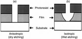
Etching: Etching is the process of selectively removing material from the wafer. After photolithography, the resist pattern protects certain areas; etching clears out the unprotected areas. There are 2 main types of etching: Wet etching and Dry etching.
In wet etching a liquid chemical, usually an acid like hydrofluoric acid (HF) is used. During fabrication, silicon wafers often have a thin silicon dioxide layer that forms. By covering parts of the wafer with resist and dipping it in HF, the exposed oxide areas are dissolved, while areas under the mask stay intact. One challenge wet etching faces is that the liquids often undercut the resist and dissolves everything that is not protected.
Due to this reason dry etching is the preferred type of etching. In dry etching, plasma is used to bombard the wafer, the plasma reacts chemically with the materials and forms volatile by products which can easily be removed. The plasma acts as a scraper and helps to remove selective material.
Etching must be very carefully controlled – if you etch too much, you might dissolve layers that were meant to stay, and if you don’t etch enough, the pattern won’t fully form. It’s a balance of selectivity (etching the target material just enough) and anisotropy (etching downward without sideways undercut).Deposition (Chemical Vapor Deposition): After etching or whenever we need to add new material layers, deposition is used. Deposition means covering the wafer with a very thin film of a material. These materials can be insulators, metals, or even additional semiconductor layers.
The most common method of deposition is Chemical Vapor Deposition(CVD), in this method one or more reactive gases are released into a chamber with the wafer under high temperature. The gas molecules then decompose when they come in contact with the hot wafer surface, leaving behind a solid byproduct which is the new material layer, and a gaseous byproduct which is then removed.
Recent Trends and Innovations and Challenges in Semiconductors
Recent trends and innovations include:
AI and Machine Learning in Process Optimization: As processes get more complicated, companies are using AI to analyze the massive data from manufacturing. Similarly, in materials R&D, machine learning can go through chemical composition possibilities much faster than trial-and-error experiments, speeding up innovation greatly.
New Semiconductor Materials: Researchers are now exploring a post-silicon future, instead of 1 material for all services, researchers are now exploring the possibility of specialized materials for each service. For example GaN-based transistors in smartphone chargers can switch at high frequency, making the charger smaller and more efficient, this is one of the reasons new chargers don’t get as hot as the old ones. 2D semiconductors like graphene are another exciting possibility though we are still some time away from achieving them.
However, the semiconductor field faces significant challenges:
Purity and Defect Control: Semiconductors are so sensitive that even the tiniest impurity or defect can ruin a device. Manufacturers go to great lengths to grow near-perfect silicon crystals and keep them pure. A 300 mm silicon wafer might contain literally trillions of atoms, yet it’s expected to be almost defect-free across its entire area which is incredibly difficult.
Control of Chemical Processes: With billions of transistors on a chip, uniformity is key. When you dope or etch or deposit, it must happen evenly across a large wafer. Uneven distribution in film thickness or dopant dose can mean some chips on the wafer perform differently or fail. This is challenging because chemical processes can depend on things like temperature, gas flow, or pressure.
Conclusion
In this post we learnt about the materials and some key processes used in making semiconductors, but this doesn’t even scrape the surface of how complex and interesting semiconductor manufacturing is. In the next post we’ll go through the step by step process of semiconductor manufacturing.


